
The Kirin 980 chipset represents a massive technological improvement over its predecessor, but it’s tiny – at just 74.13mm², it’s a good 30% smaller than the Kirin 970. That’s one of the advantages of the 7nm process. But looking at the die shot (taken by ChipRebel), the CPU and GPU with all their cores take up less than half of the chip.
The 980 is the first chipset by HiSilicon to use ARM’s new DynamIQ technology, which makes it easier to build heterogeneous designs. The DSU – DynamIQ Shared Unit – is the heart of the system. Connected to it are two different pairs of Cortex-A76 cores.
They run at different clock speeds – 2.6GHz and 1.92GHz – and their different designs suggests they have been optimized to run at those speeds. This is much more efficient than simply ramping up the clock speed of one pair. The four small A55 cores and the 4MB of L3 cache hook up to the DSU as well.
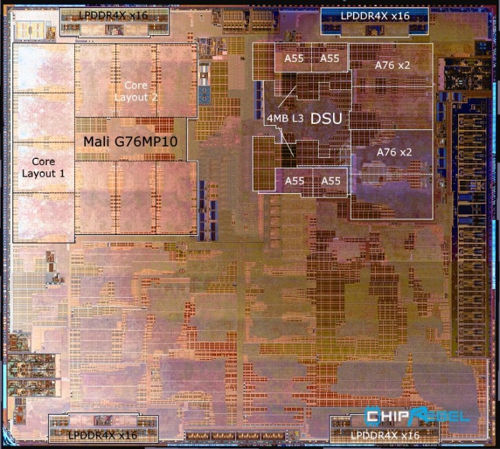
Off to the left is the new Mali G76 MP10 GPU, which promised 50% higher performance than a G72. Our benchmarks show that it didn’t deliver on that promise, in fact it was fairly even with the Mali-G72 MP12 of the older Kirin 970.
Somewhere in this complicated mix of transistors that is the Kirin 980 is the dual core NPU, which Huawei claims is more than twice as fast as the original NPU in the 970. You also see the LPDDR4X RAM controllers, this chipset is the first to support 2,133MHz memory.
[“source=cnbc”]